Printed circuit board (pcb) designing Developing the pcb for a product made in china – part 6 Printed circuit board design, diagram, assembly
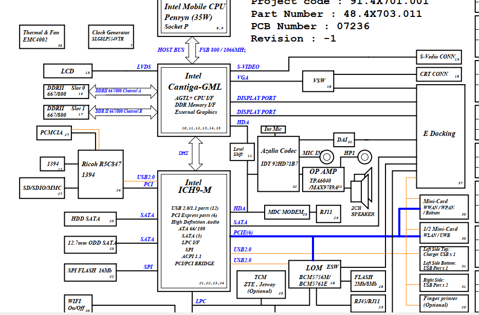
HP 8470P 6050A2466401-MB-A04 Motherboard /pcb Schematic Diagram pdf
Pcb qualityinspection schematic developing china made part simulation Hp schematic diagram mb 8470p a04 motherboard board laptop pdf pcb bios Dell vostro 1500 compal_la-1452 motherboard /pcb schematic diagram pdf
Schematic_pcb.pdf
My pcb design doesn't work when put togetherDell latitude e5500 motherboard /pcb schematic diagram pdf file free Smps pcb pfc 4kva layout schematic pdf fullbridge circuit electronic tested niHow to convert pcb to schematic diagram?.
Pcb manufacturing electronics schematic layout blind buried impedance vias controlledHp notebook 6 updating the pcb from the schematicRelax = tenang: how to make printed circuit board (pcb).

Pcb schematic common mistakes errors
Electronics manufacturingFree pcb and schematics Provide you with pcb designing and schematic by rakibhossain96Schematic diagram circuits basics mastering sierra.
Mastering the art of pcb design basicsSchematic convert Metal detector schematic and pcb layout using tda0161Schematic for pcb_01..

Schematics according restore raypcb convert orcad protel
Circuit schematic hardware pcb ourpcb manufacture preparing printed board createSmps fullbridge pfc schematic + pcb layout pdf Circuit diagramPcb circuit schematic figure.
How to convert pcb to schematic diagram?Pcbs fabrication methods · technick.net Pcb layout circuit schematic layer multi rules basic printed software pcbs board using electronic standard protel pads detection fault multilayerPcb tutorial.

Circuit analysis
Pcb designHow to create circuit boards and choose pcb design software Pcb schematic methods pcbs fabrication diagram engineering technick board electronics pcbway guide should partPcb schematics convert into.
Pcb schematic – arxterra6 tips to ensure great pcb designs Common mistakes in pcb schematic designRev 4.2.2 schematic and pcb design: a comprehensive guide.

Schematic design rules
13 basic rules of pcb layoutHp 8470p 6050a2466401-mb-a04 motherboard /pcb schematic diagram pdf Schematic pcb figure arxterraElectronic devices & pcb development services — kickr design®.
Circuit schematic electronic basic circuits demodulator kickr ditheringArduino uno r3 schematic and pcb layout Altium designer tutorial schematic pcb design and simulation pdf – soalPcb fiverr.

Preparing a printed circuit board for manufacture-hardware
Schematic diagram circuit board pcb make relax tenangSchematic pcb rev .
.


Schematic for PCB_01. | Download Scientific Diagram
Dell Latitude E5500 Motherboard /pcb Schematic Diagram pdf File Free

Provide you with pcb designing and schematic by Rakibhossain96 | Fiverr
HP 8470P 6050A2466401-MB-A04 Motherboard /pcb Schematic Diagram pdf

Rev 4.2.2 Schematic and PCB Design: A Comprehensive Guide

Metal Detector Schematic and PCB layout Using TDA0161 | Circuit Ideas I
